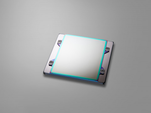
Image of EUV lithography with pellicle, a protective film for the photomask (Photo: Business Wire)
Dai Nippon Printing Co., Ltd. (DNP, TOKYO: 7912) has begun development of a photomask manufacturing for 2-nanometer (10-9 meter) generation logic semiconductors that support Extreme Ultra-Violet (EUV) lithography, the cutting-edge process for semiconductor manufacturing.
DNP will also act as a subcontractor and provide the newly developed technology to Tokyo-based Rapidus Corporation (Rapidus). Rapidus is participating in the Research and Development Project of the Enhanced Infrastructures for Post-5G Information and Communication Systems instigated by the New Energy and Industrial Technology Development Organization (NEDO).
[Background]
We have strengthened our ability to manufacture cutting-edge semiconductors with high productivity and quality. And in 2016, DNP was the world’s first merchant photomask manufacturer to introduce the multi-beam mask writing tool (MBMW) (https://cts.businesswire.com/ct/CT?id=smartlink&url=https%3A%2F%2Fwww.global.dnp%2Fnews%2Fdetail%2F20167043_4126.html&esheet=53912205&newsitemid=20240319148117&lan=en-US&anchor=the+world%27s+first+merchant+photomask+manufacturer+to+introduce+the+multi-beam+mask+writing+tool+%28MBMW%29&index=1&md5=21574a3a0234c50c11329836bda06de4).
In 2023, we completed the development of a photomask manufacturing process for 3-nm generation EUV lithography (https://cts.businesswire.com/ct/CT?id=smartlink&url=https%3A%2F%2Fwww.global.dnp%2Fnews%2Fdetail%2F20170124_4126.html&esheet=53912205&newsitemid=20240319148117&lan=en-US&anchor=the+development+of+a+photomask+manufacturing+process+for+3-nm+generation+EUV+lithography&index=2&md5=7130ba412c110f525c8568434719b854), and commenced development of 2-nm generation technology. In response to the need for further miniaturization, we will begin full-scale development of a photomask manufacturing process for 2-nm generation EUV lithography, including the operation of second and third multi-electron beam mask lithography systems in FY 2024.
DNP plans to bring online its second and third MBMW mask lithography systems in FY 2024, accelerating the development of photomasks for 2-nm generation EUV lithography.
DNP will act as a subcontractor on Development of Advanced Semiconductor Manufacturing Technology (Commissioned) by Rapidus as part of the NEDO’s previously mentioned R&D project.
[Going Forward]
By FY 2025, DNP will complete the development of a manufacturing process for photomasks for 2-nm generation logic semiconductors that support EUV lithography. From FY 2026 onwards, we will push ahead with the establishment of production technology with a view to commencing mass production in FY 2027.
We have also begun development with an eye toward the 2-nm generation and beyond, and have signed an agreement with imec, a cutting-edge international research organization headquartered in Leuven, Belgium, to jointly develop next-generation EUV photomasks. DNP will continue to contribute to the growth of Japan’s semiconductor industry by promoting development in collaboration with various partners within the framework of the international semiconductor industry.
More Details (https://cts.businesswire.com/ct/CT?id=smartlink&url=https%3A%2F%2Fwww.global.dnp%2Fnews%2Fdetail%2F20173706_4126.html&esheet=53912205&newsitemid=20240319148117&lan=en-US&anchor=More+Details&index=3&md5=9c42839f0bbbe19a11b90b1169239385)
About DNP
DNP was established in 1876, and has become a leading global company that leverages print-based solutions to engineer fresh business opportunities while protecting the environment and creating a more vibrant world for all. We capitalize on core competencies in microfabrication and precision coating technology to provide products for the display, electronic device, and optical film markets. We have also developed new products, such as vapor chamber and reflect array that offer next-generation communication solutions for more people-friendly information society.
View source version on businesswire.com: https://www.businesswire.com/news/home/20240319148117/en/
언론연락처: Dai Nippon Printing Co., Ltd. Yusuke Kitagawa +81-3-6735-0101
이 뉴스는 기업·기관·단체가 뉴스와이어를 통해 배포한 보도자료입니다.HD현대의 조선 부문 중간지주사인 HD한국조선해양이 선박 전동화를 위해 전력 반도체 세계 1위 기업인 독일 인피니언과 손을 잡았다.
HD한국조선해양은 최근 경기도 성남시에 위치한 HD현대 글로벌R&D센터(GRC)에서 독일 인피니언 테크놀로지스(Infineon Technologies AG)와 ‘선박 전동화 기술 공동 개발을 위한 상호협력 협약(MOU)’을 체결했다고 28일(목) 밝혔다.
이번 협약식에는 HD한국조선해양 장광필 미래기술연구원장과 인피니언 테크놀로지스 아시아퍼시픽 비벡 마하얀(Vivek Mahajan) 부사장 등이 참석했다.
HD한국조선해양은 강화되고 있는 환경 규제에 대응하기 위해 선박 전동화를 적극 추진 중으로, 선박 전동화에 필요한 전력 반도체 관련 기술 확보를 위해 전력·차량용 반도체 분야의 세계적인 기업인 인피니언과 협력하기로 했다.
전기추진 선박은 엔진 대신 전동기가 생산한 출력으로 움직이는데, 전동기의 출력을 안정적으로 제어하기 위해 ‘추진 드라이브’가 장착된다. 전력 반도체는 추진 드라이브의 전력 변환과 제어를 담당하며, 추진 드라이브의 성능과 신뢰성을 결정짓는 핵심 부품이다.
이번 MOU를 통해 인피니언은 HD한국조선해양이 선박 추진 드라이브 개발에 필요한 전력 반도체 기술을 지원한다. 또 필요 시 추진 드라이브에 최적화된 전력 반도체를 공동 개발하고, 선박 분야 전동화 관련 기술 교류를 진행할 계획이다.
HD한국조선해양과 HD현대중공업은 현재 외산 제품에 의존 중인 추진 드라이브의 국산화를 위해 최근 한국전기연구원(KERI)과 공동 개발에 착수한 바 있다. 이 추진 드라이브는 MMC(Modular Multilevel Converter) 전력회로를 기반으로 해 대용량·고전압 계통에 특화된 것이 특징이다.
HD한국조선해양 장광필 미래기술연구원장은 “조선업과 전력 반도체 세계 1위 기업 간의 협력을 통해 전동화 핵심 기술을 확보함으로써 선박 전동화를 선도해 나가겠다”고 말했다.
한편 HD현대는 지난해 그룹 내 전동화 연구조직들을 통합해 글로벌R&D센터(GRC)에 전동화센터를 개소하고, 전동화 분야의 세계적인 석학인 설승기 서울대학교 교수를 전동화센터 기술자문위원으로 위촉했다. HD현대 전동화센터는 선박, 건설기계 분야의 전동화 선행 기술과 핵심부품 개발 연구 등을 수행하고 있다.
 속초19.1℃
 24.7℃
24.7℃